The Role of Photonics in AI: Advancing Speed and Efficiency
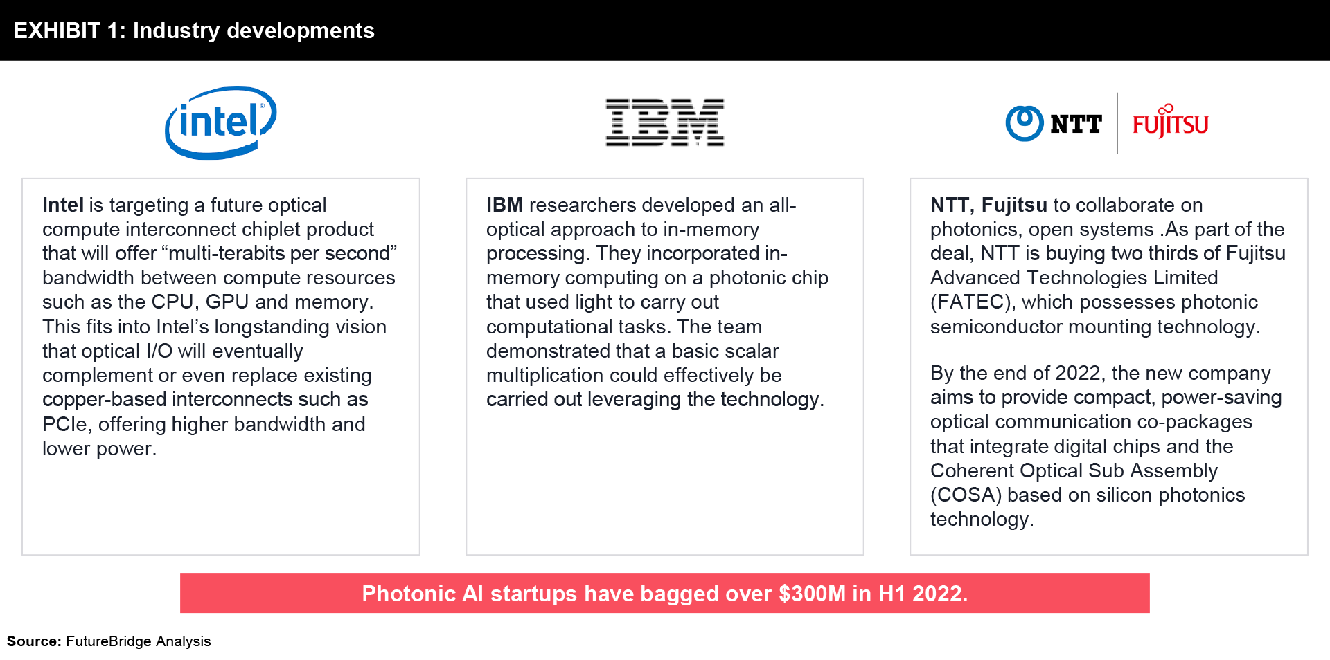
With the rapid advancements of AI and ML applications, a quickly developing marketplace for processors that can better accelerate neural network workloads is flourishing. However, the power required and slow transmission of electronic data between the processor and the memory is limiting complex operations with greater accuracy by current digital processors suitable for deep learning, such as graphics processing units or tensor processing units. We are still far from biological counterparts with current electronic implementations of neuromorphic architectures. To address this, Photonics in AI is being explored to reduce the hardware pain points in computing. Compared to electronics, optical technology has the distinct advantages of both lower power and lower latency, which are two elements with particular significance to AI. Optical approaches to AI acceleration have recently gained more interest due to the innovative advantages of photonics, such as high bandwidth, low power consumption, and efficient data movement. Industry leaders such as IBM, Intel, and HP are investing billions of dollars in the transition to photonics in AI.

State of Art: Photonic AI Accelerators
Researchers at Monash University in Melbourne and RMIT have developed advanced photonic circuits that can change the speed and scope of photonics technology. A single fingernail-sized chip can transmit 39 terabits per second according to the paper published in nature.
Earlier in 2020, George Washington University researchers demonstrated the use of a photonic processor to carry out mathematical operations. They experimented with a photonic TPU to perform mathematical operations foundational for training neural networks, specifically matrix multiplication. This processor could perform many operations in parallel via wavelength division multiplexing: the use of different wavelengths of light to run multiple signals on a single optical fibre. However, the chip consumed 80W of power and its performance (in terms of operations per joule) was estimated to be two to three orders of magnitude higher than a conventional electrical TPU with similar chip areas. Switching from electronic to optical hardware can reduce the energy consumption of AI models considerably.
In July 2020, the Department of Defence of the United States closed solicitations with an objective to develop high-speed, scalable, power-efficient photonic accelerators for vector, matrix, and tensor operations with potential applications in artificial neural networks.
Earlier in 2019, IBM and Oxford researchers presented a photonic computational memory for direct scalar multiplication of two numbers, using a single integrated photonic memory change cell. Their device relies on the distinct interaction of two pulses, both of which represent a number to be multiplied. The researchers are working to figure out how to neatly scale-up matrix sizes on photonic chips.
In 2019, MIT research suggested that photonic chips could run optical neural networks 10 million times more efficiently than their electrical counterparts.
Startups like Lightelligence are developing optical chips that empower the next generation of high-performance computing tasks. By processing information with light, its chips offer ultra-high-speed, low latency, and low power consumption which has not been possible in traditional electronic architectures.
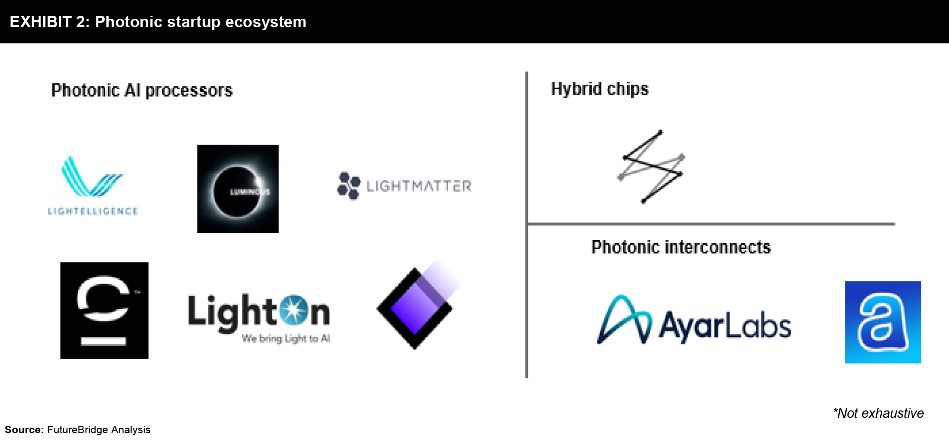

Another Paris-based startup LightOn is also accelerating efforts to develop optical computing for Machine Learning. Lightmatter, Optalysis, and Fathom Computing are other startups vying for a slice of the budding optical chip market and have raised tens of millions in venture capital for their own chips.
Ayar Labs intends to commercialize its chip-to-chip optical photonics technology, which it claims is a much faster way to transmit data than electrical signaling while using much less power. Ayar Labs and Hewlett Packard Enterprise (HPE) have collaborated to develop silicon photonics solutions based on optical I/O technology.
Commercializing photonics
- The majority of current commercial applications use photonics just for communications across racks in the data center.
- Standalone photonic AI accelerators for enabling edge computing applications for IoT. E.g., Cognifiber
- Startups like Salience Labs combine an ultra-high-speed multi-chip processor that packages a photonics chip together with standard electronics.
- Application-specific photonics chip – the University of Pennsylvania in the US has developed a remarkably scalable 9.3mm square microchip able to both detect and classify an image in less than a nanosecond.
The continued rise of cloud computing and artificial intelligence will drive technological breakthroughs, enabling rapid advancement and commercialization of silicon photonic chips.
Photonics further extends to application-specific use cases
Integrated Photonics is an Application Specific Photonic Integrated Circuit (ASPIC). Unlike traditional PICs, which are more general-purpose devices, ASPICs are optimized to perform specific functions in terms of propagation loss, power consumption, footprint, and component count. Compared to PIC, ASPIC tends to offer much better performance for certain applications due to its special nature.
However, application-specific photonics poses some technical and logistical challenges. To address some of these challenges, photonic computing company iPronics is developing software-programmable photonic processor technology. In July 2022, iPronics made headlines when the company successfully raised $3.7 million in funding to accelerate the launch of its technology for an industry-first software-reconfigurable general-purpose photonics processors.
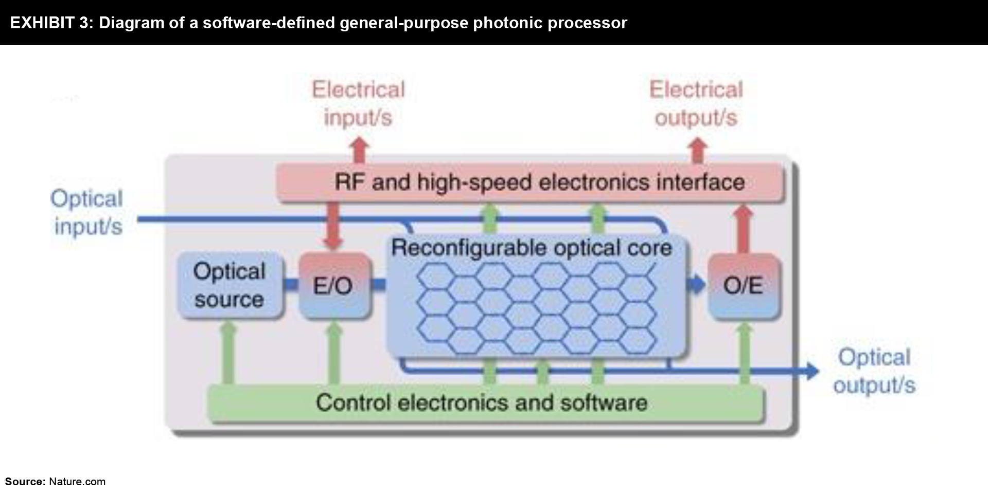

Programmable ASPIC helps democratize the adoption of PIC technology by allowing engineers with no hardware or photonics experience to design their own products.
The Future of Photonics in AI
Wearable photonics is a promising candidate to complement wearable electronics in complex systems.
Medium-infrared photonics show promise for applications ranging from environmental monitoring, healthcare monitoring, and industrial inspection. It is conceivable that photonic neural networks integrated with photonic sensors in a monolithic fashion can perform AI functions such as on-chip learning and recognition. In this way, data can be processed on-chip and only a small amount of important data is eventually sent to the cloud server to reduce the requirement of high computing power in the AIoT era.
Optical computing is not the only technique that can possibly address the hardware pain points of current AI models. Other technologies that might help improve the speed and efficiency of AI models are quantum computing and neuromorphic chips. Moreover, Photonics won’t be replacing the Electronics market but, deliver functionalities that can’t be achieved with electronics.
The combination of energy efficiency, near real-time latencies, and scalability would potentially make optical computing suitable for a variety of AI environments – from hyper-scale clouds to IoT edge devices. But first, the technology will have to prove itself to be generally viable, and if so, the kind of application domains that would make the most sense for it should be identified.
Reach out today to discuss how we can collaborate. Contact us for your business inquiry and let’s explore new opportunities together!


